Artists get all the good stuff first.
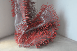
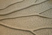
When the University of Manchester published a paper on the properties of the wonder-material graphene on Thursday, the ears on Trebuchet’s art team pricked up. Graphene, still very much a subject for scientific study, is already old news in the art world, as evinced by GV Art’s current exhibition, Graphite.
[GV Art’s] partnership with the National Graphene Institute allows them to show the recently discovered wonder-material, graphene, as part of their enquiry into the nature of graphite’ (From Trebuchet events).
Writing in Nature, Nobel Prize-winner Professor Kostya Novoselov and an international team of authors has produced a ‘Graphene Roadmap’ which for the first time sets out what the world’s thinnest, strongest and most conductive material can truly achieve.
One key area is touchscreen devices, such as Apple’s iPad, which use indium tin oxide. Graphene’s outstanding mechanical flexibility and chemical durability are far superior. Graphene touchscreen devices would prove far more long-lasting and would open a way for flexible devices.
The authors estimate that the first graphene touchscreen devices could be on the market within three to five years, but will only realise its full potential in flexible electronics applications.
Rollable e-paper is another application which should be available as a prototype by 2015 – graphene’s flexibility proving ideal for fold-up electronic sheets which could revolutionise electronics.
Timescales for applications vary greatly upon the quality of graphene required, the report claims. For example, the researchers estimate devices including photo-detectors, high-speed wireless communications and THz generators (for use in medical imaging and security devices) would not be available until at least 2020, while anticancer drugs and graphene as a replacement for silicon is unlikely to become a reality until around 2030.
The paper also details the different ways of producing graphene – processes which have evolved hugely from the sticky tape method pioneered by the Nobel Laureates.
The paper asserts that there are three main methods for making graphene:
Liquid phase and thermal exfoliation – exposing graphite to a solvent which splits it into individual flakes of graphene. This method is ideal for energy applications (batteries and supercapacitors) as well as graphene paints and inks for products such as printed electronics, smart windows and electromagnetic shielding. Adding additional functionality to composite materials (extra strength, conductivity, moisture barrier) is another area such graphene can be applied.
Chemical Vapour Deposition – growing graphene films on copper foils, for use in flexible and transparent electronics applications and photonics, among others.
Synthesis on Silicon Carbide – growing graphene on either the silicon or carbon faces of this material commonly used for high power electronics. This can result in very high quality graphene with excellently-formed crystals, perfect for high-frequency transistors.
Professor Novoselov said: “Graphene has a potential to revolutionise many aspects of our lives simultaneously. Some applications might appear within a few years already and some still require years of hard work.
Source: University of Manchester

The aim of art is to represent not the outward appearance of things, but their inward significance. – Aristotle


